Surface imperfections refer to various processing defects, such as pitting, scratches, open babbles, broken edges, broken spots, ect.
They are on the polished surface, and mainly caused by processing or subsequent improper operations.
Today we will introduce 4 types of surface defects.
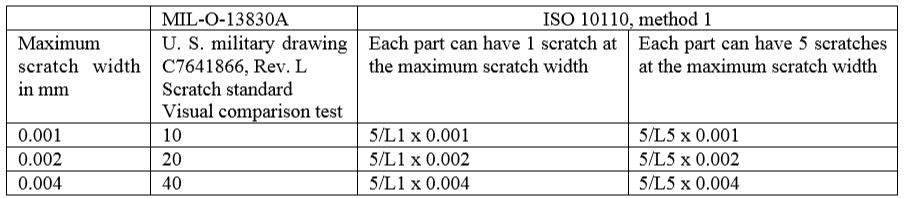
Scratch means long linear marks on the surface of optical elements.
Due to the length of the scratch, it can be divided into long scratches and short scratches.
Based on 2mm, if scratch less than 2mm, it is a short scratch, otherwise is long scratch.
For short scratches, the evaluation criteria are the cumulative length at which they are detected. Relatively speaking, scratches are easier to detect than defects such as pitting.
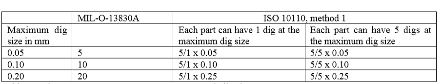
2- Dig or Pitting
Digs, pits, eched pits, are often interpreted in linear dimesion by its diameter with unit of 1/100 mm.
Digs have close width and depth, and the edges are often irregular.
In general, a defect with an aspect ratio greater than 4:1 is scratched, whereas a defect less than 4:1 is a dig.
In ISO standard, N x A means dig requirement.
N is number of digs at maximun size, A is the maximum size of each digs in mm.
While in Din 3140 standard, use "K" indicate scratch.
Below is a table for dig:
3- Broken edge/Edge chips
It is a defects on the edge of optical elements, it's often outside the effective area of the light source, but may also cause light scattering, cause cosmetic and functional concerns.
In ISO standard, EA''' means edge chip requirement.
E is the header for edge chip, A''' is the maximum chip size from the physical edge of the surface in mm.
In Din3140 standard, use "R" indicate edge chips.
4- Surface contaminants
It means small dirts, coating spots, splash point and so on.
In general, they can not remove by air bubble, alcohol or acetone.
They may remove by re-polishing.
In Din3140 standard, use "C" indicate coating defects or other contaminants.
Surfact defects can hardly affect the optical system and damage other optical elements.
1- Lower the quality of light beam.
The defect area may cause light beam scatter, the energy of beam is greatly consumed after passing through the defect.
2- Thermal effect.
The defect area is easy to absorb more energy, the thermal effect phenomenon may cause local deformation of the element, damage the coating layer, ect.
3- Damage other optical elements.
In optical system, the scattered light beam can be absorbed by other elements, which may over the threshold of elements material and cause serious damage to the system.
For surface defect standards, LPO normally use ISO10110, MIL-13830 and Din 3140.
If you need more info, please check LPO Resources page or contact us!


